Transmission Line analysis
Characterization of transmission lines in microelectronic circuits using a Maxwell solver
Modeling and characterization of electromagnetic wave interactions with microelectronic devices to derive network parameters has been a widely used practice in the electronic industry. However, as these devices become increasingly miniaturized with finer-scale geometric features, computational tools must make use of manycore/GPU architectures to efficiently resolve length and time scales of interest.
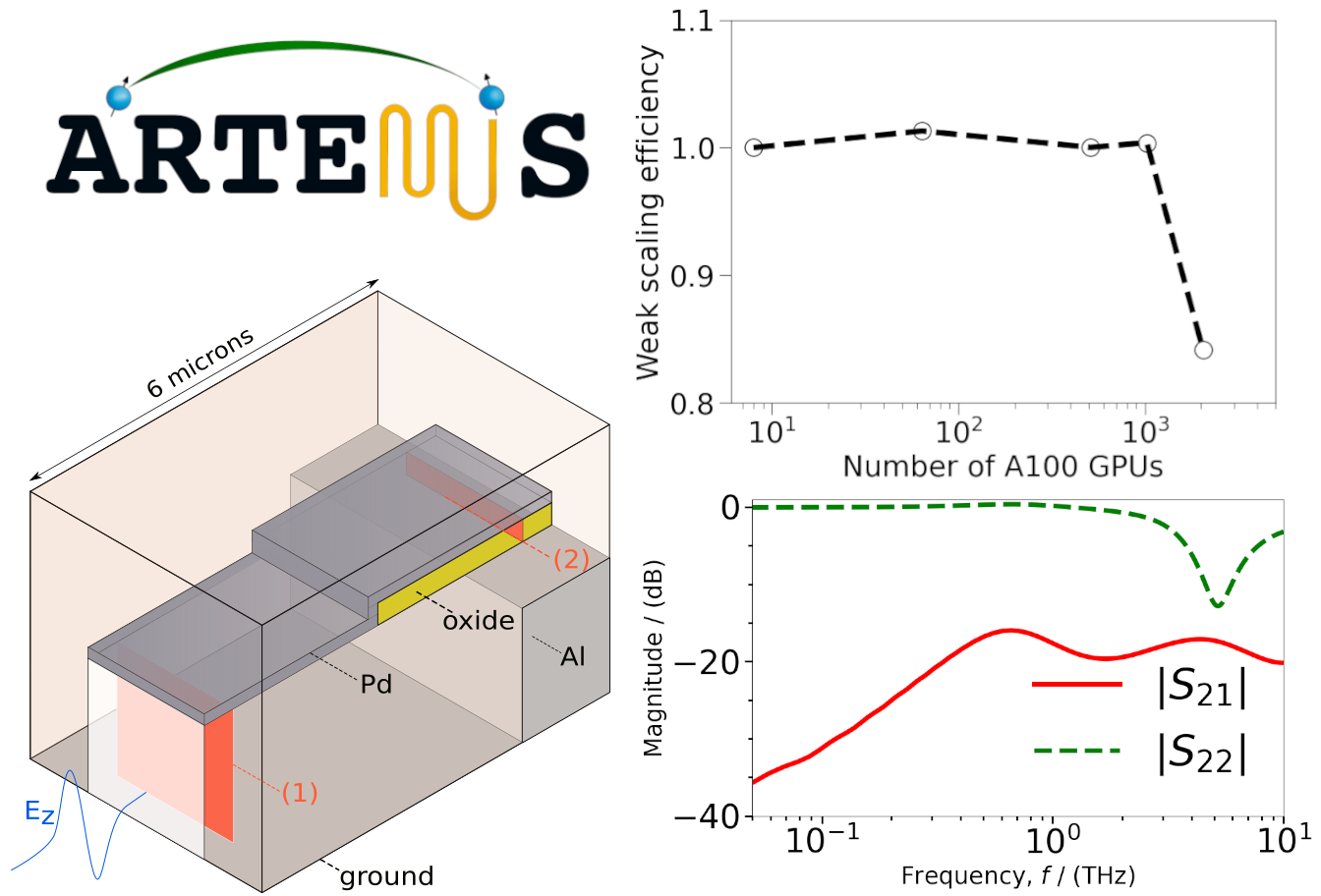
This has been the focus of our open-source solver, ARTEMIS, which is performant on modern GPU-based supercomputing architectures while being amenable to additional physics coupling. This work demonstrates its use for characterizing network parameters of transmission lines using established techniques. A rigorous verification and validation of the workflow is carried out, followed by its application for analyzing a transmission line on a CMOS chip designed for a photon-detector application. Simulations are performed for millions of timesteps on state-of-the-art GPU resources to resolve nanoscale features at gigahertz frequencies. The network parameters are used to obtain phase delay and characteristic impedance that serve as inputs to SPICE models. The code is demonstrated to exhibit ideal weak scaling efficiency up to 1024 GPUs and 84% efficiency for 2048 GPUs, which underscores its use for network analysis of larger, more complex circuit devices in the future. For details, please see (Sawant et al., 2022).

Left: A microscale transmission line with a Z-directional electric field excitation for computing S-matrix between ports (1) and (2). Bottom Right: Components of S-matrix as a function of frequency. Top Right: Weak-scaling efficiency of ARTEMIS on NVIDIA A100 GPUs using NERSC's Perlmutter supercomputer.